Antenna Report
Antenna rules are part of the DRC.
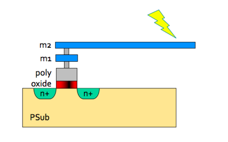
When the ASIC is being built up layer by layer, we have the gates of the MOSFETS built first. Then we use the metal layers to connect them into bigger blocks. The metal layers are etched using a plasma which is made of ionised atoms, and the electrical charge from this can build up on already existing wires. The more static charge that builds up, the higher the voltage that is seen. If some part of the wiring attaches to a transistor gate, then the voltage may be high enough to cause that gate to be destroyed - this is similar to a charge building in clouds and finally a lightning bolt (spark) can break through the air. The antenna rule controls the ratio of metal area to gate area because this reflects the amount of voltage that may build up and the size of the gate over which the strain needs to be borne. If there is a diode in the same part of the wiring then this will act to drain away charge and so it increases the lmit on the ratio between metal and gate by a large amount.
After LibreLane finishes, we have an antenna report in this file: ./reports/routing/41-antenna.rpt (number may change with LibreLane config)
The antenna report is a long collection of smaller reports like this:
  _1438_  (sky130_fd_sc_hd__clkbuf_1)  A
[1]  met2:
  PAR:   36.40  Ratio:    0.00       (Area)
  PAR:  182.35  Ratio: 3134.60       (S.Area)
  CAR:  115.98  Ratio:    0.00       (C.Area)
  CAR:  582.45  Ratio:    0.00       (C.S.Area)

[1]  met1:
  PAR:   79.50  Ratio:    0.00       (Area)
  PAR:  400.02*  Ratio:  400.00       (S.Area)
  CAR:   79.58  Ratio:    0.00       (C.Area)
  CAR:  400.10  Ratio:    0.00       (C.S.Area)

[1]  li1:
  PAR:    0.07  Ratio:    0.00       (Area)
  PAR:    0.09  Ratio:   75.00       (S.Area)
  CAR:    0.07  Ratio:    0.00       (C.Area)
  CAR:    0.09  Ratio:    0.00       (C.S.Area)

[1]  M1M2_PR:
  PAR:    0.34  Ratio:    6.00       (Area)
  CAR:    0.49  Ratio:    0.00       (C.Area)

[1]  L1M1_PR_MR:
  PAR:    0.15  Ratio:    3.00       (Area)
  CAR:    0.15  Ratio:    0.00       (C.Area)
We have the name of the net, in this case ‘1438’.
Then 5 subsections related to the layers of the chips that each have a PAR or CAR value on the left and a ratio on the right. PAR and CAR refer to Partial or Cumulative Antenna Ratio.
From this reference on page 375:
- A PAR tells you if any single metallization step is likely to inflict damage to a gate.
- A CAR adds the damages on successive layers together to accumulate them as the layers are built up.
If the value exceeds the ratio then it’s a violation. This is shown by an asterisk (grep ‘*’ 41-antenna.rpt to find all the violations).
So in the report above we can see we have an antenna violation on met1 as the PAR value of 400.02 exceeds the ratio of 400.
Ignoring antenna violations
On the skywater slack, Tim Edwards recently spoke about this:
The general principle here is that antenna violations will give you a yield hit—that’s something to worry about on a production run because it will affect profit margins. But for a test chip on an MPW run, you could in principle have a yield loss as high as 10% and never notice it. So then it comes down mostly to personal choice. If the antenna violation is in a circuit that you think people will re-use as-is on other projects, then it would be in your best interest to knock the antenna violations down to zero. But it is most likely that the antenna violations occur in (1) a synthesized block which would most likely be resynthesized if re-used in another project, or (2) a top level layout which would necessarily be re-done for another project. That’s the thinking behind my guidance.
And:
Most violations are not worth fixing unless they exceed the ratio by 2x
LibreLane automatically inserts antenna diode cells to protect nets. Note that adding diodes increases the net capacitance and may slow signals down. As this addition of diodes happens late on in the flow, there is a risk that it will degrade timing.
There is another way to fix antenna rule violations - by adding jumps to higher metal layers in the middle of a large ‘antenna’. For instance, if a section of metal2 is causing a violation, then breaking it in half and jumping to metal3 for a short distance, or doing this near the gate(s) that are at risk, means that the antenna size on metal2 attached to the gate is reduced. It may also mean that by the time all of the original metal2 wiring is in the section of the net attached to the gate, that also some diode will also be attached and hence the charge will be drained away anyway.
LibreLane no longer supports DIODE_INSERTION_STRATEGY, instead using 2 flags, GRT_REPAIR_ANTENNAS and RUN_HEURISTIC_DIODE_INSERTION. For more information, check the LibreLane docs.
LibreLane summary tool
The LibreLane summary tools can list antenna violations with the –antenna flag
Course feedback
The course helped me to understand how digital designs are produced in industry. If you're interested in electronics, take this course - I mean it's an amazing course!
Andrey (digital course)