Corner
MOSFET characteristics can vary across multiple wafers.
If we wanted to make sure a sensitive analog design worked across all process variations, we would want to simulate these variations and check the results were still within our specification.
Some of the most common variations affect the strength or speed of the MOSFET switching, and we have both P and N type MOSFETS. The corners represent the most extreme variations of these parameters. By combining them, we get these combinations:
- FF (fast fast)
- SF (slow fast)
- SS (slow slow)
- FS (fast slow)
- TT (typical typical)
In practice, libraries also have custom corners apart from these combinations. These take things like aging, parasitics, leakage, etc. into account.
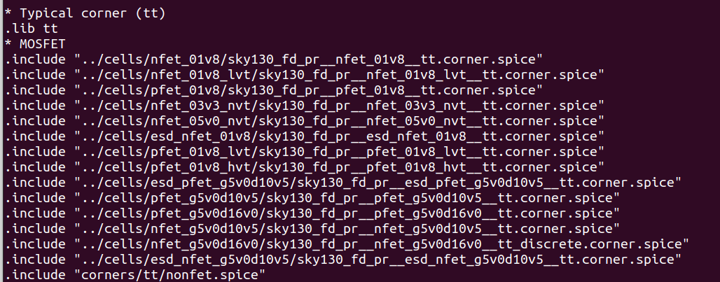
We have SPICE models of the different corners provided in the Skywater PDK.

Fast transistors are ones that can switch more than typical current, and thus charge up attached capacitances more quickly which will make the voltage on wires switch faster. The two main factors that make a transistor faster are reducing the gate length, which means etching the polysilicon gate slightly narrower, or changing the doping. If both the P and N transistors are formed by the same etching step then they are likely to both be thinner (or fatter) than typical together, but the doping of P and N are done separately so there is no reason for the two to vary in the same way. This means that FF,TT and SS corners are more likely to happen than the ‘skew’ cases of SF or FS which require the P and N devices to vary from typical in opposite ways.
Process corners may combine two separate elements: the modelling of the transistors, and the modelling of wiring parasitics. As the transistors and wiring are made in totally separate process steps, the transistors on a particular chip may have fast transistors but large parasitics which will tend to slow signals down. The ‘fast’ corner typically combines fast transistors and low parasitics, the ‘slow’ corner combines slow transitors and large parasitics.
To truly know whether a design will function under all real-life conditions, designers normally check for process, temperature and voltage variations. The slowest conditions are typically SS process corner, low power supply voltage, high temperature. The faster conditions are typically FF process corner, high power supply, low temperature. To find the highest clock rate your design is likely to work at, you probably need to analyse under the slow conditions. To find ‘hold time’ violations - where signals shoothrough logic earlier than expected and cause failures - you typically need to analyse under the fastest conditions. For analog circuits it may not be obvious which are the worst case set of conditions, so the designer may need to verify under different settings of process, temperature and voltage.
For my basic simulations, I often remove all the corner libraries except TT, to speed up the simulation time.
For more information, check this Wikipedia page: https://en.wikipedia.org/wiki/Process_corners
Course feedback
Having the formal verification part additionally felt nice, that I could have something that I know is going to be functional instead of just guessing for a long time and then looking at waveforms and then not knowing what hell I'm doing!
Dylan Wadler (digital course)