Wafer
Silicon is purified to around 99.9999999%! Then it is sliced into very thin round sheets called wafers.
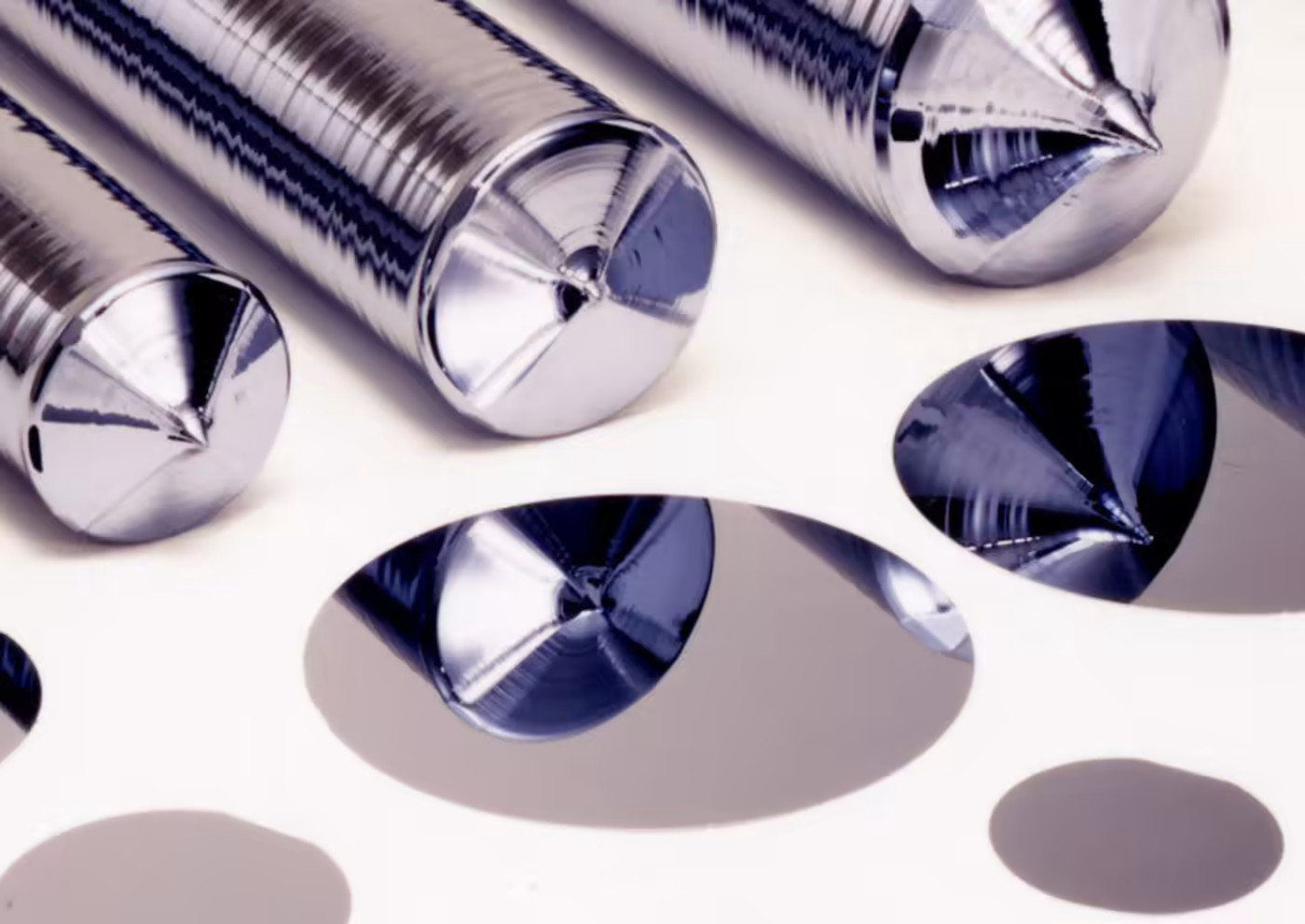
The type used in the Skywater 130nm process is doped to become p-type.
Here’s a great video about how silicon wafers are made.
And these great videos are about the birth of the Japanese semiconductor industry. Jump to about 12 minutes in to see how they pull the silicon ingot out of the molten material.
After the wafers are ready, they can be patterned using the photolithographic process, using a series of masks.
Course feedback
Anybody who wants to learn about ASIC design who's never done it, this was a great introduction. I really enjoyed the course, this has been a great learning experience.
Tom Gwozdz (digital course)