Maskset
From Wikipedia:
A photomask is an opaque plate with holes or transparencies that allow light to shine through in a defined pattern. They are commonly used in photolithography and the production of integrated circuits (ICs or “chips”) in particular. Masks are used to produce a pattern on a substrate, normally a thin slice of silicon known as a wafer in the case of chip manufacturing. Several masks are used in turn, each one reproducing a layer of the completed design, and together they are known as a mask set.
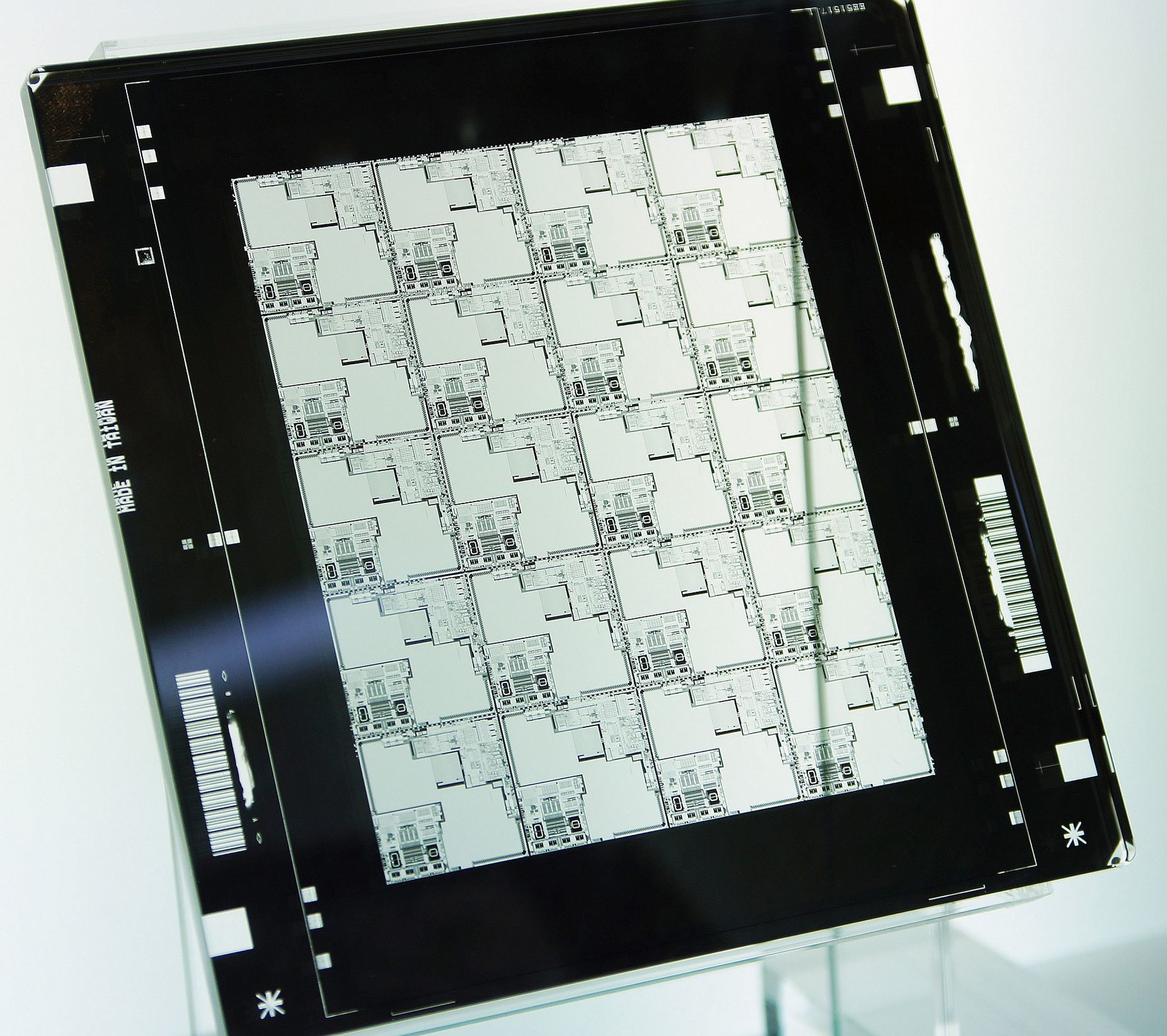
This mask shows 20 copies of the same design, so a single exposure (in the stepper) will create the pattern for 20 chips. The mask is made from fused quartz (instead of glass) and the pattern is made by depositing chrome evenly on the surface of the quartz and removing it using lasers or ion beams. The pattern on the mask is typically 5 times larger than the image projected onto the wafer, this optical reduction allows the mask to be cheaper to produce and makes dust on the mask less significant (because its shadow will also be shrunk by a factor of 5. The whole maximum exposed area on the wafer on a given step is typically 25mm across, the pattern on the mask is thus 125mm across.
In the case of the Skywater PDK, we have 33 different layers and so 33 different masks are needed. The masks have to be extremely precisely made, which is why the whole set of masks ends up being so expensive. You can see a list of all the layers and what they are used for on this spreadsheet.
For experimentation, a Multi Project Wafer is often used to lower the costs.
The process of using the masks to create the patterns on the silicon wafer is called photolithography.
Course feedback
It’s a fairly daunting prospect going into something like an ASIC, but I feel confident now that I could pick another project up and go from the start with the Verilog and end up with something that will hopefully work.
Jamie Iles (digital course)