MPW
A Multi Project Wafer is used to reduce the cost of making an ASIC. By using a lot of different designs on the same wafer the Non Recurring Engineering (NRE) costs of making the mask set are shared between all the participants.
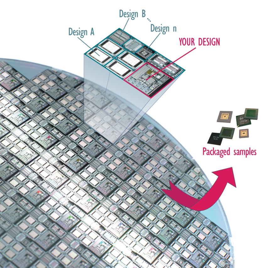
The Google shuttle is an example of an MPW.
Our MPW submissions
So far we have made 4 tapeouts to the Google MPWs:
MPW physical implementation
We sent John McMaster some chips to take a look at from MPW1. Here presented his findings at OpenTapeOut
And you can browse his microphotographed die here
Course feedback
The course itself is very self sufficient, and on top of that you have the community behind it. People are happy to help and review your work. I would definitely recommend the course!
Louis Ledoux (digital course)