MPW
A Multi Project Wafer is used to reduce the cost of making an ASIC. By using a lot of different designs on the same wafer the Non Recurring Engineering (NRE) costs of making the mask set are shared between all the participants.
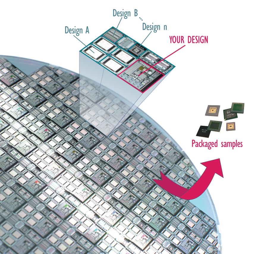
The Google shuttle is an example of an MPW.
Our MPW submissions
So far we have made 4 tapeouts to the Google MPWs:
MPW physical implementation
We sent John McMaster some chips to take a look at from MPW1. Here presented his findings at OpenTapeOut
And you can browse his microphotographed die here
Course feedback
It was such a great opportunity to do something on my own and see a piece of silicon where there is my invention or my part doing things. It was in the back of my mind for a long time, I think it was my dream to put something into silicon but it was so expensive until this opportunity arrived.
Pawel Sitarz (digital course)