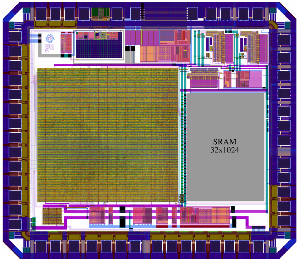
Padring
We need to make sure we can package the IC after the wafer has been diced into individual dies.
A common way of packaging ICs is to connect them to a leadframe by bonding tiny wires between the leads of the leadframe and the pads on the die.
The big bond pads around the outside of the IC often include ESD protection diodes, Input/Output drivers and so on.
This picture shows raven, an IC from Efabless. You can see around the edge there are the big bond pads and the power and ground lines. This structure is called a padring.
The padring used in the Google shuttle is included in Caravel.
Course feedback
I can highly recommend the Zero to ASIC course, especially to other students. Thanks to the grant program I was able to get a Silicon Level ticket and actually fabricate my own chip. It was a great opportunity to take something I learned at university in my case, Huffman coding and implement it in real silicon. The course made the whole process understandable and achievable.
Marvin B (digital course)