Photolithography
Sam Zeloof did a great talk about his home IC foundry at the Hackaday Supercon 2019.
This slide shows an overview of the process:
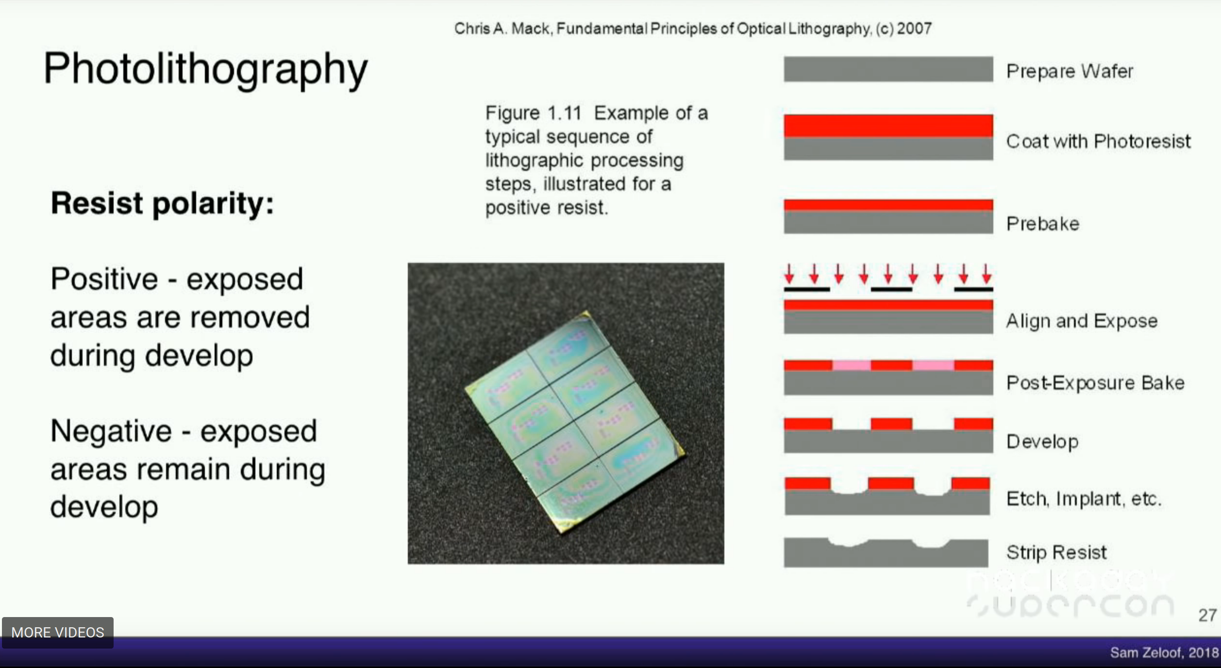
A series of masks is used to build up a 3 dimensional structure on the wafer.
Each step is fundamentally the same:
- Deposit a layer of silicon dioxide (glass) on the surface of the wafer
- Coat the glass with photoresist (which is a light sensitive organic compound, similar to photographic emulsion)
- Bake it
- Use a mask to cover certain areas and use light (often UV) to illuminate the areas not covered
- Develop the photoresist, which will wash out the areas exposed. This leaves holes through to the glass
- Etch the glass through the holes in the resist - this turns the glass into a ‘hard mask’
- Strip away the remaining photoresist
- Now use the hard mask to control where the next step can take effect, for instance we could implant dopants to change the electrochemical properties. The dopant will reach the silicon beneath only where there are holes in the hard mask. Or we can etch away underlying metal (in older aluminimum processes), or in modern copper processes grow metal in the trenches in the glass.
- If no longer need the hard mask, strip it away and repeat the whole process for the next layer up.
Photolithography is the key that allows us to take the patterns we create in a tool like Magic or LibreLane and miniaturise them down to the nanometer scale. It also lets us easily tile the same design over the wafer to make the individual dies. It allows us to use a prepared image of the chip to make millions of copies reliably and rapidly.
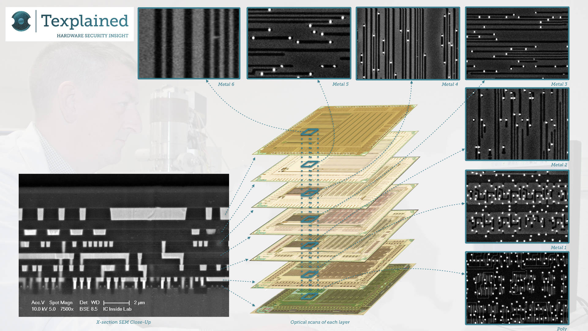
This cross section shows how the layers are used to build up the 3 dimensional structures that make up the IC.
Course feedback
A great course to really learn about Analog ASICs and electronics in general, great material and support community.
Diego Satizabal (analog course)