Shuttle
A shuttle service is the same as a multi project wafer.
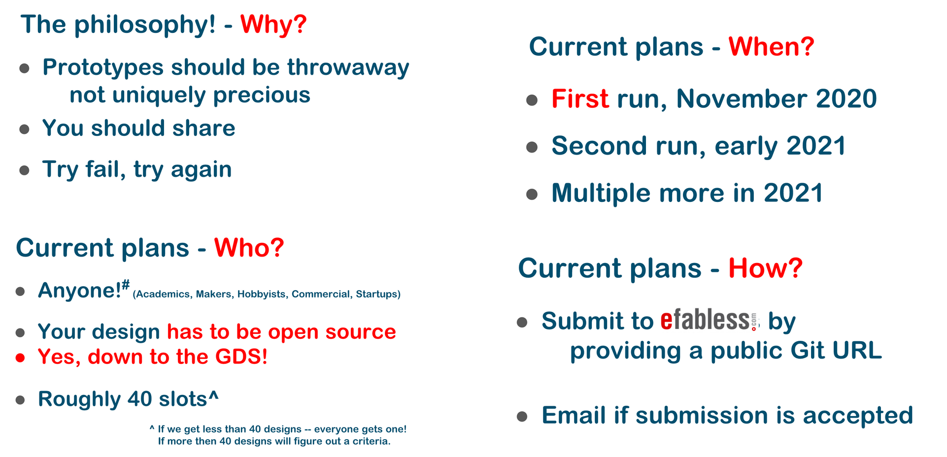
On 30th June 2020, Tim Ansell announced the collaboration between Google and Skywater to provide a free shuttle service in his FOSSI dialup talk.
These slides taken from his talk show the overview:
Chip Foundry Shuttle
Normally in an MPW you would have the whole die to yourself. In the ChipFoundry Shuttle all the designs will be within the user project area of the Caravel harness.
Caravel has its own RISCV processor and a neat datasheet. The idea here is to make it easier to bring up and debug your designs at the cost of some area.
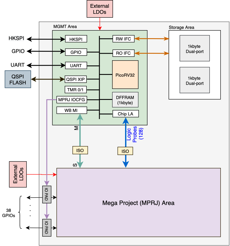
Read this post to find out what you could fit in the user space.
The Google shuttle returned chips in type of packaging called Wafer Level Chip Scale Packaging and then the easier to handle QFN.
Course feedback
The Zero To ASIC course took me on a fantastic journey from drawing and simulating a MOSFET, formal verification leading up to implementing a custom design with an open PDK and completely open source tools. The course is crammed full of interesting material with great pacing and support from Matt, and it's been a fantastic opportunity to meet other folks with shared interests and different backgrounds. The course has left me excited with opportunities for new projects and optimism for some working silicon!
Jamie Iles (digital course)