MPW1 Bringup
I submitted my first ASIC designs to the free Google shuttle in December of 2020.
In October 2021, we heard there were serious clock related problems with the management area of the chip due to issues with the toolchain. It seemed unlikely that anyone would be able to get anything beyond a single blinking LED from MPW1. The hold violations in the management system meant that the PicoRV32 cpu couldn’t run and setup the GPIOs. So even if our designs work, we can’t get access to them.
Chips received!
Efabless shipped our bumped dies as well as bare dies and I received mine on the 24th of January 2022.
![]()
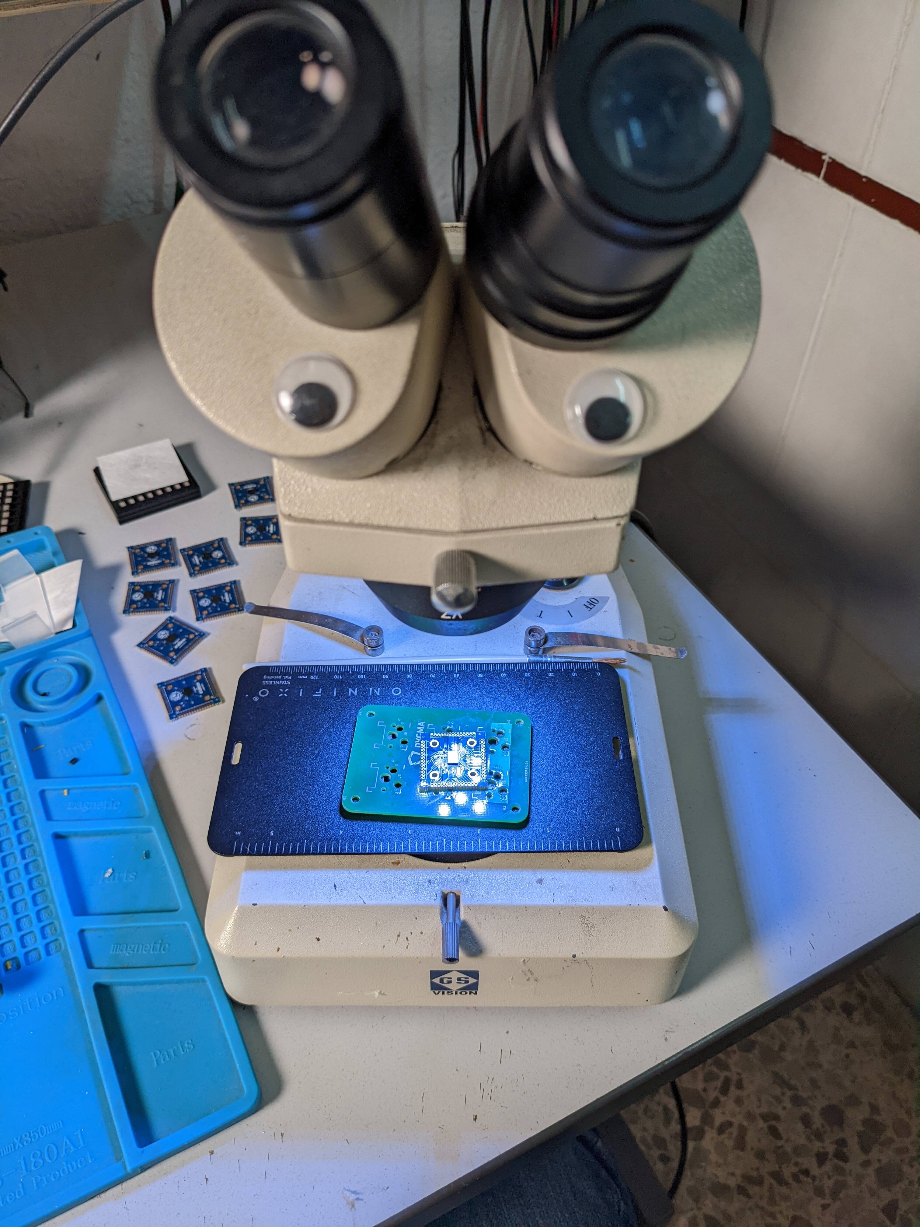
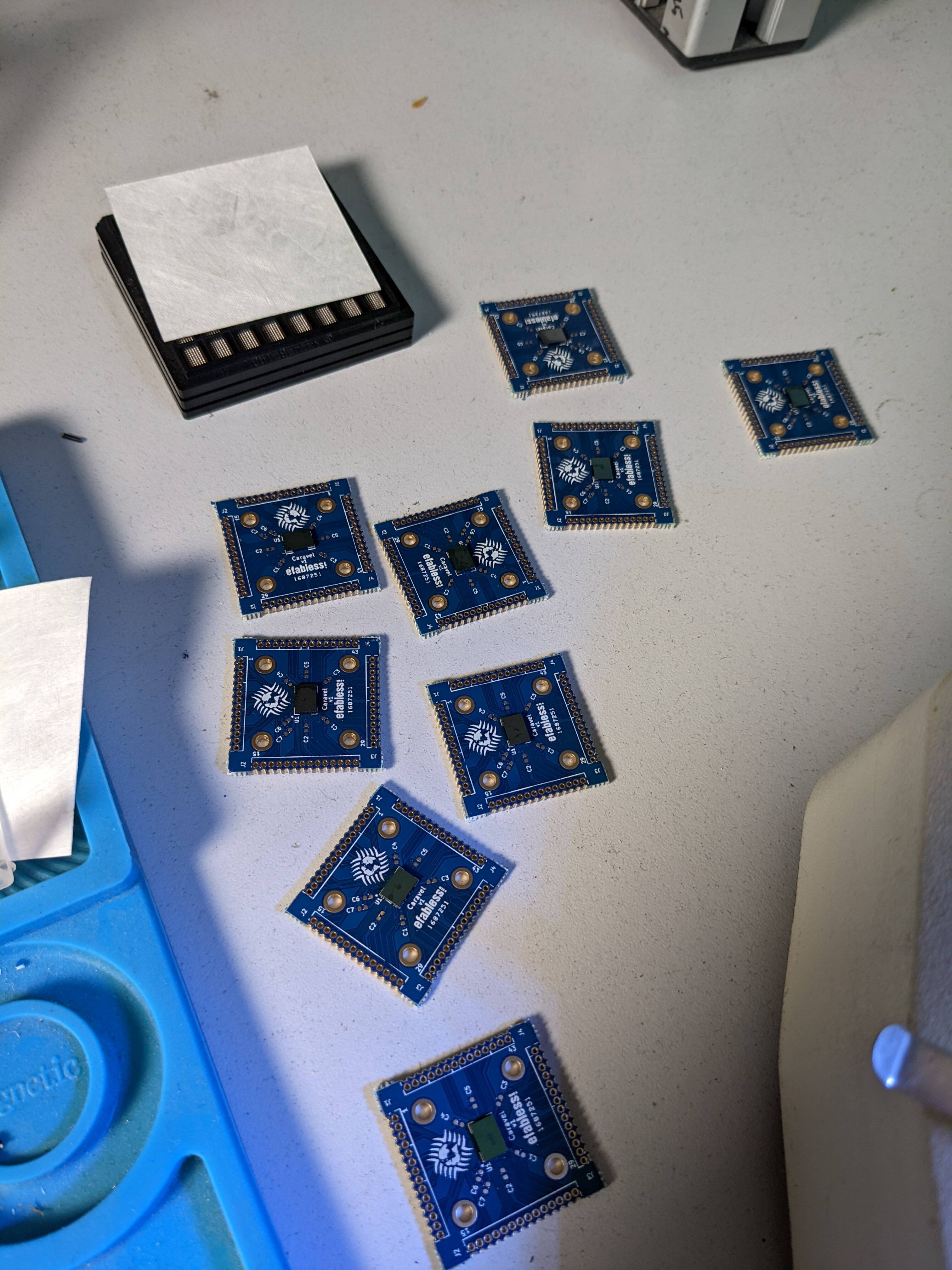
As well as the chips, we also received some handy breakout boards. So the first step was doing some careful soldering to mount 10 of the chips on the breakouts. This was done with flux and hot air.
Post mortem board
Hacker extraordinaire tnt had also submitted a design to MPW1, which we spoke about in this interview. He has worked with the Michael Welling of QwertyEmbedded to get a ‘post mortem’ board designed and made.
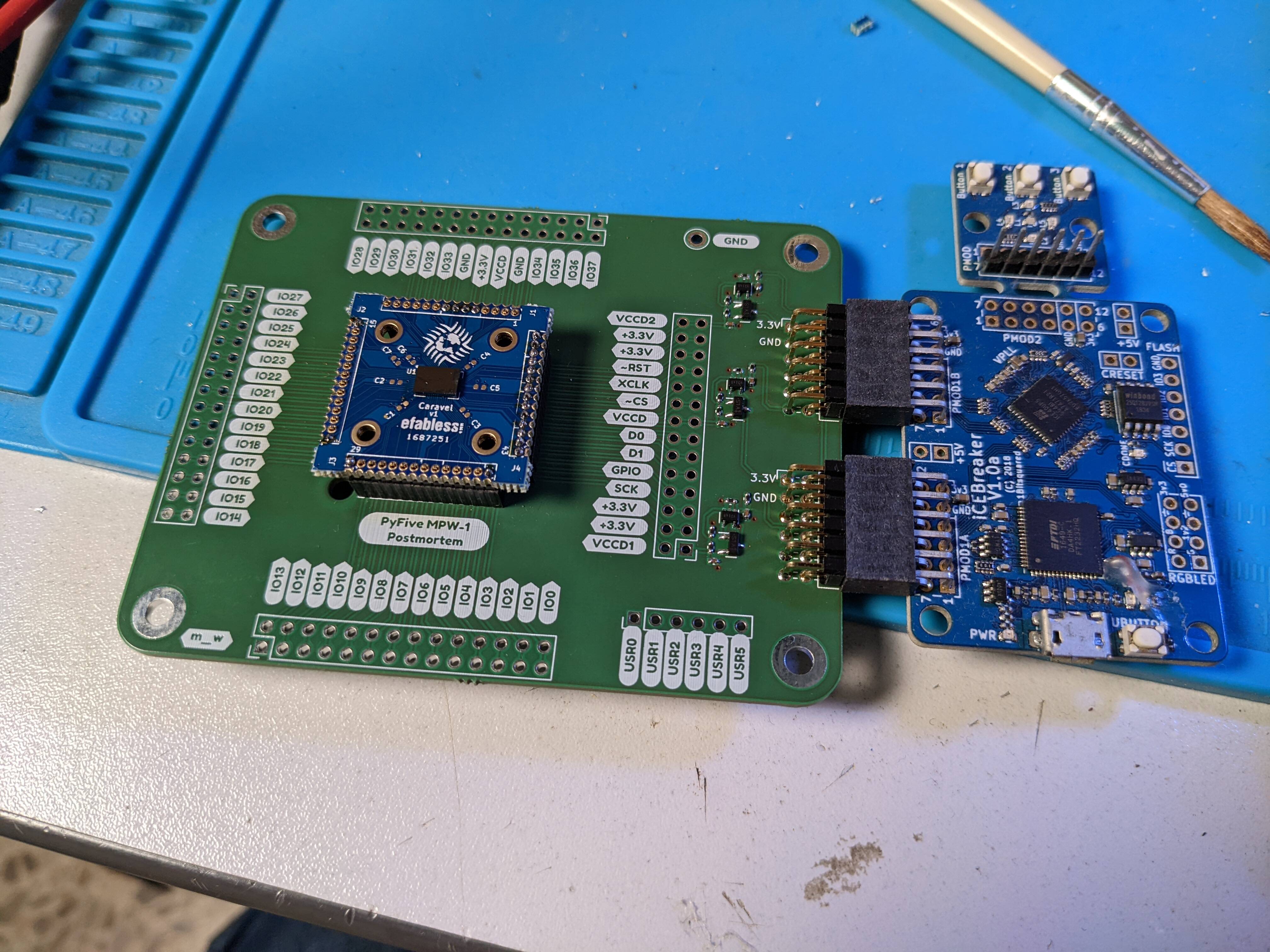
The board allows easy access to the pins and provides 3 adjustable voltage rails. An icebreaker FPGA board allows us to control the voltage supplies and also provide the firmware by simulating a FLASH chip.
Board repository here.
The idea is to use a script to measure the number of sucessful FLASH reads the PicoRV32 can make before it hangs. Then the script changes the voltage by a few mV and continues. After we scan the range of voltages, hopefully we find one where the PicoRV32 can run for a few thousand instructions. Out of 10 chips I found 3 that were worth further testing.
Signs of life
The default project on my chips is the 7 segment seconds counter. We loaded some special firmware to set the IOs to outputs and one of the outputs started toggling!
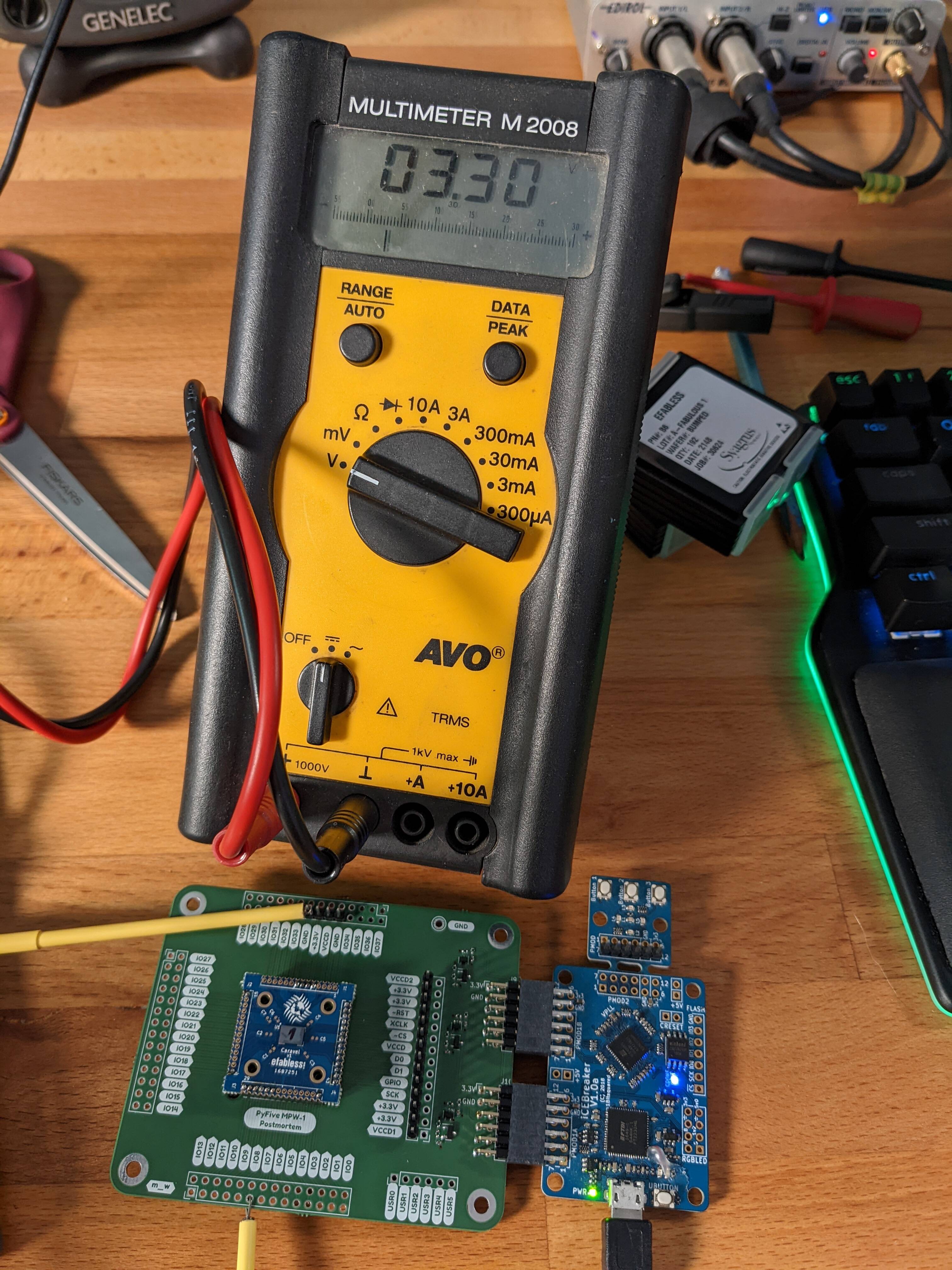
5 segment counter!
After some fettling we were able to get 5 out of the 7 IOs set to outputs.
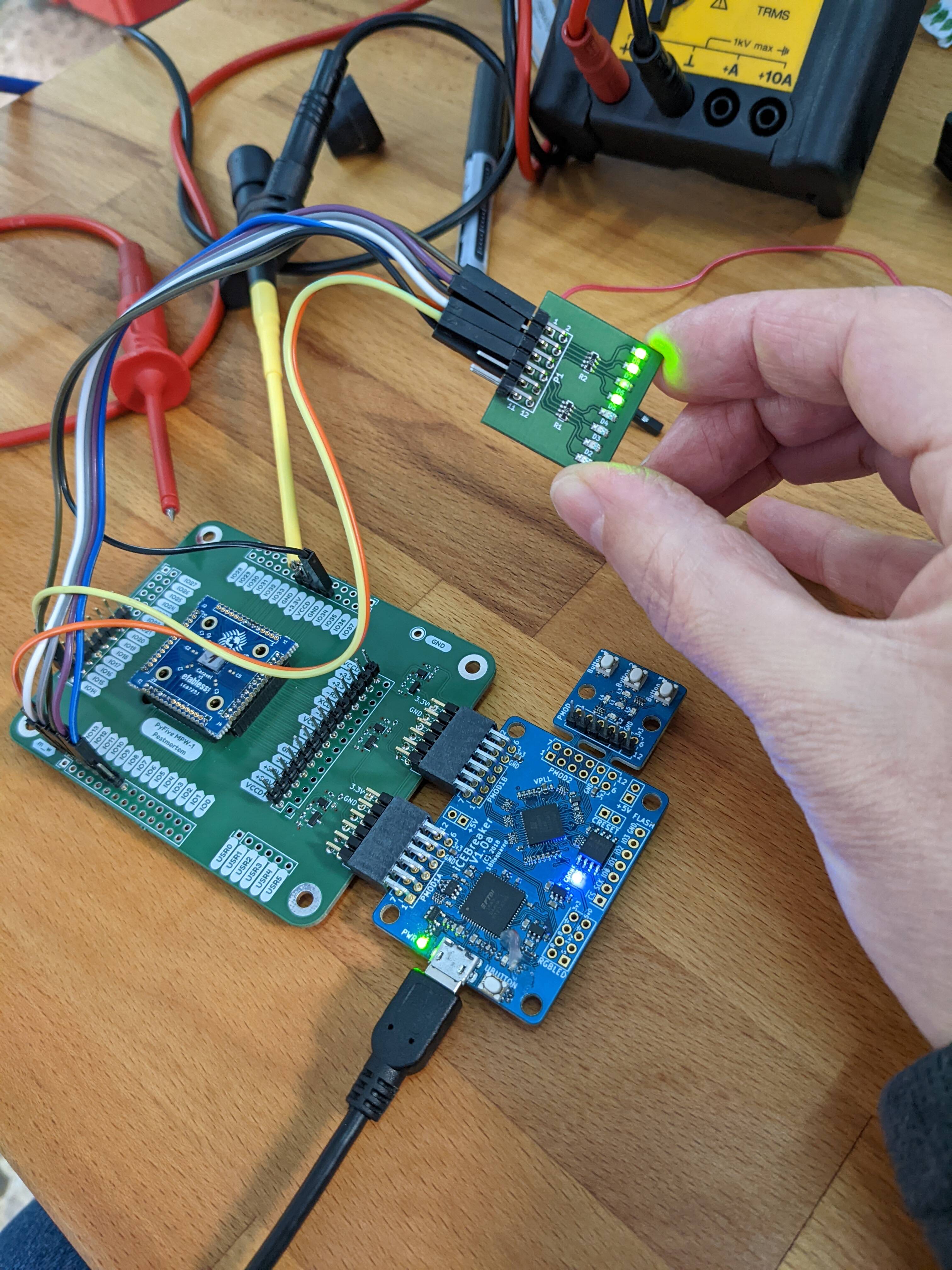
I’m pretty confident with some more work I’ll be able to get all 7 segments working, but even if that doesn’t happen it still feels amazing to have my own chips in hand, running my own designs.
It’s also great to see that the multiplexing of the projects worked, that the OpenLane tools worked well enough to create a working design.
Lots of room for improvement obviously, but great validation of the whole process.
Next steps
Another thing to try is the chip’s built in logic analyser. If I can get this to work I can select another design to be active. There are 8 designs in total, and I’d like to try the WS2812 driver and VGA clock design too.
The repository I’m using to document the process is here: https://github.com/mattvenn/mpw1-bringup
Learn more
tnt has a video showing his own chips (kind of) working here.
And he’ll be documenting his bring-up methodology soon, so make sure to subscribe (and like! and ring the bell!).
Make your own!
If you want to learn to design your own chips and get them made, check out my course!